Wafer Inspection & Metrology
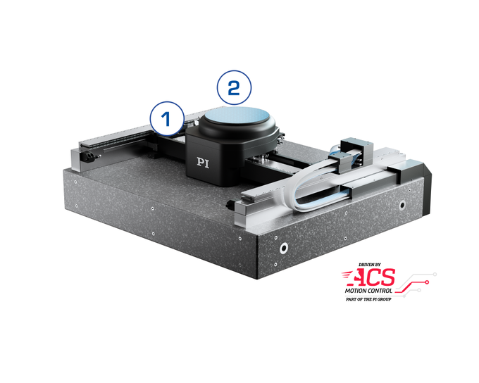
Highly Dynamic and Precise Piezo Wafer Positioning Solutions
Efficient wafer inspection and metrology are essential in semiconductor manufacturing to prevent yield loss. Achieving this requires precise wafer positioning, which enables fast and reliable analysis of defects and particles at every production stage.
PI’s cutting-edge piezo wafer positioning solution outperforms traditional electromagnetic systems with its innovative design, advanced control capabilities, and seamless connectivity. Featuring a dual-function piezo actuator, hybrid kinematics, and next-gen motion controller, the system delivers unmatched precision and reliability. The solution corrects wafer misalignment, maintains precise positioning, and eliminates heat generation by operating energy-free in a static state. Dynamic piezo adjustments ensure flatness and angular error compensation, guaranteeing consistent focus accuracy.
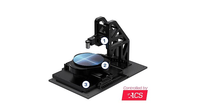
The stage design shown and described here is a demonstrator based on proven technologies. Similar systems have already been successfully implemented in customized solutions. Please feel free to contact us if you would like to explore how we can support your specific application requirements.
Z Axis - Dynamic Tracking
- Piezo motor technology
- Power off holding ability
- High resonant frequency enables highly dynamic tracking and correction mode for fine motion.
- Travel range: up to 4 mm coarse and 50 µm fine
- Move-and-settle time <10 ms (0.01 µm - 50 µm)
- Bidirectional repeatability: 10 nm (1 sigma)
- Position stability <5 nm
θZ Axis - High-Accuracy Motion
- Piezo motor technology
- High resonance frequency for highest stability
- Travel range: up to ±6 mrad for highest accuracy, can be extended to up to 360°
- Move-and-settle time <20 ms (0.1 µrad - 100 µrad)
- Bidirectional repeatability: 0.5 µrad (1 sigma)
- Position stability <0.05 µrad
Advantages
Our hybrid piezo wafer stage concept offers several advantages. Piezo motors are inherently stiff, self-clamping and can hold a position without power. They do not introduce additional servo jitter, and the high stiffness and bandwidth can be used for dynamic tracking or compensation of external disturbances and instabilities. With move and settle times down to <10 ms and position stability of <5 nm and <0.05 µrad, respectively, this new piezo wafer stage combines ultra-high performance with excellent value.
Dynamic Operation
The newly developed piezo wafer stage from PI offers significant advantages over electromagnetic concepts. With native support for wafer fiducial alignment, before positioning/moving the wafer, the module first corrects the rotational misalignment of the wafer and holds the wafer in the correct position under the tool. Wafer thickness and machine static characteristics are taken into account.
Once the process is complete, the actuators can be turned off and held in position so that no more energy is needed, and therefore, no heat is generated in the wafer area that could affect precision. This eliminates the need for additional cooling or balancing.
The secondary mode of the piezo actuators is used to locate and track the focus. The analog element mode allows for highly dynamic operation, compensating for flatness and angular errors and ensuring that the focus is maintained.