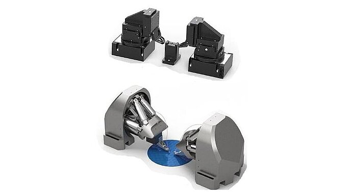
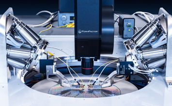
Integrating photonic components, such as waveguides, lasers, photodiodes, and multiplexers, onto a silicon chip introduces numerous testing challenges, not only at the wafer level. From conceptualization to series production, a substantial volume of performance data for each element is essential for successfully conveying the structure's design and ensuring its qualification. Given the significant process costs involved in SiPh chip production through final packaging, early identification of defective chips is imperative. This early detection allows for their removal from the manufacturing process, thereby minimizing potential losses and optimizing the overall efficiency of the production workflow.
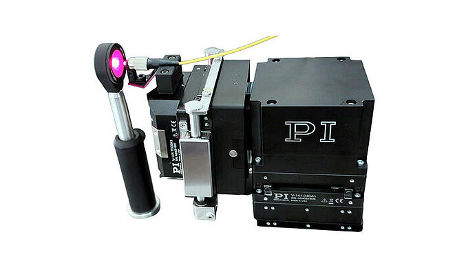
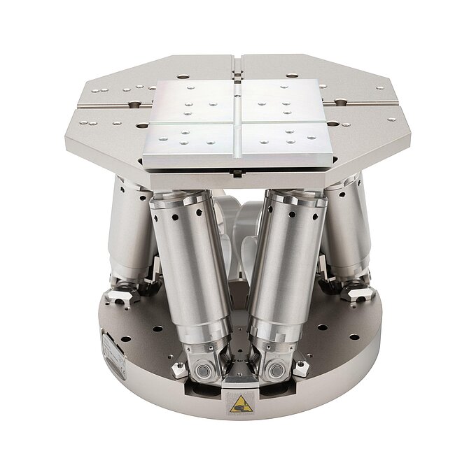
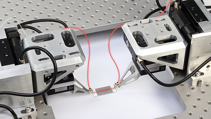
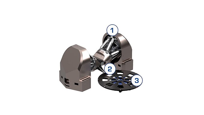
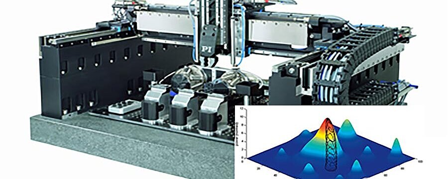
The process of automating the alignment of fibers, waveguides, fiber optic arrays, lasers etc., especially the time it takes for each alignment is a major cost driver in silicon photonics test and packaging. Automated alignment systems with PI’s advanced algorithms and mechanics are the solution to the problem – cutting down on alignment time by orders of magnitude while achieving ultralow-loss alignment performance with arrays with 0.02dB typical coupling repeatability.
