Products - PI (Physik Instrumente) L.P.
6-Axis Alignment System Provides Faster Optics & Photonics Alignment with Virtual Pivot Point and Piezo Precision
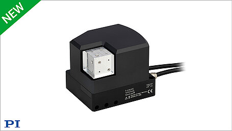


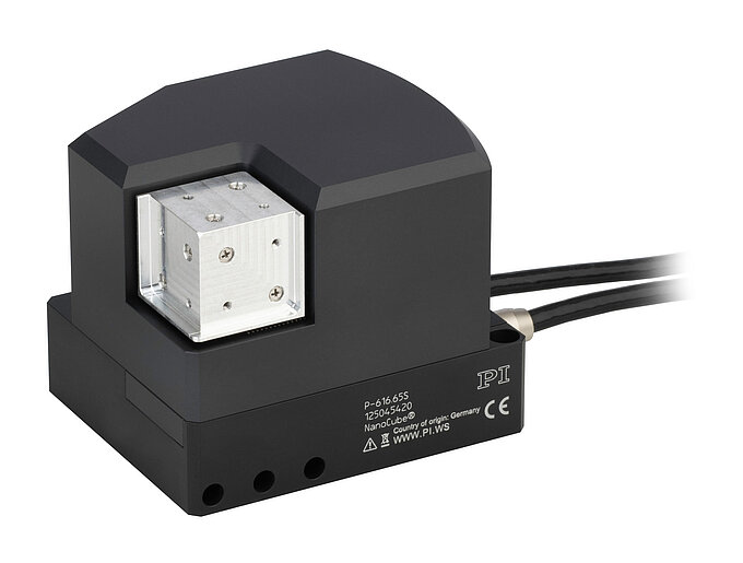
PI’s new P-616.65S 6-axis alignment system – based on a 6-DOF piezo-flexure stage – is ideal for high-speed photonics and micro-optics alignment applications. With 500µm linear travel in X, Y, and Z, a rotational range of 3° in θX, θY, θZ, and true parallel-kinematic 6-DOF motion, the novel platform establishes a new standard for compactness, dynamic performance, and precision in photonics, semiconductor, and microscopy applications. A user programmable virtual pivot point (center of rotation) and high-speed alignment routines built directly into the digital controller firmware further enhance versatility, accelerating setup and throughput.
High Stiffness = High Dynamics and Rapid Step and Settle
Its integrated, rigid, and friction-free flexure structure provides high stiffness—characterized by a resonant frequency of 350 Hz—and enables fast dynamics with rapid step-and-settle performance, ideal for fast scanning and automated multi-channel photonics alignment.
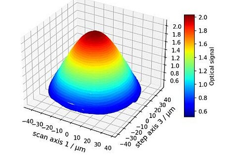
Powered by PICMA® all-ceramic actuators with demonstrated 100-billion-cycle lifetime, the system offers exceptional reliability even in 24/7 high-duty-cycle environments. Closed-loop position control with high-resolution sensors delivers nanometer-level repeatability across all motion axes.
Key Technical Highlights
- Ultra-compact 6-axis alignment system—small enough to fit in the palm of your hand.
- 500µm travel range in X, Y, and Z
- 3° rotation in θX, θY, θZ for full 6-DOF adjustment
- User-selectable pivot point—in software for intuitive multi-axis alignment
- Nanometer level resolution and repeatability for reduced insertion loss
- Parallel-kinematic flexure design for uniform stiffness and zero friction
- Compact aluminum construction, vacuum-compatible, and resistant to shock and vibration
Smart Firmware for Faster Alignment
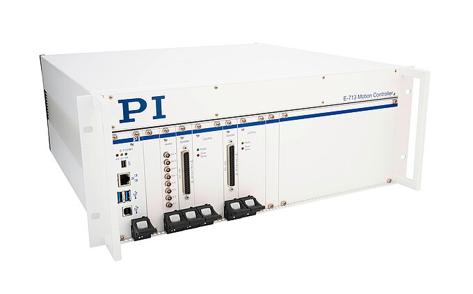
In combination with PI’s E-713 digital nanopositioning controllers the new NanoCube aligner features embedded high-speed routines for first-light detection, gradient search, coordinate scans, and multi-axis optimization. By eliminating the need for external scripts or PC-side computation, these firmware algorithms significantly shorten alignment times in production workflows.
A Compact Workhorse for Advanced Photonics
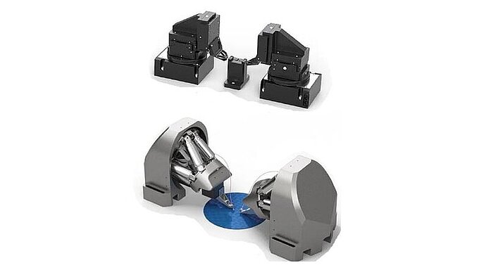
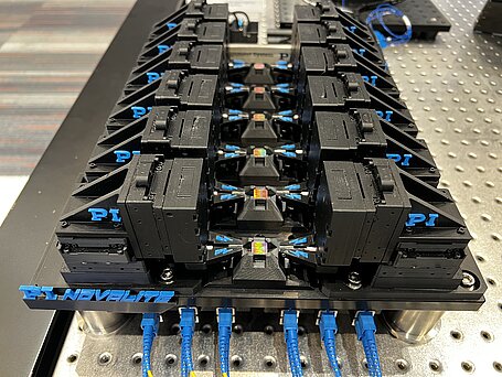
The NanoCube® complements a wide range of advanced and proven alignment solutions that PI offers to the photonics industry—from its award-winning hexapod-based FMPA system to its cost- and throughput-optimized modular PINovAlign product family. As manufacturers continue to push for smaller footprints and higher throughput, this new piezo-flexure-based solution provides a powerful tool for high-volume photonics assembly and testing.
The new NanoCube® system is available now for OEM integration, research laboratories, and fully automated photonics-alignment subsystems.
» More information on NanoCube® 6-Axis Alignment System
» More information on Alignment Controller for NanoCube® 6-Axis Alignment System
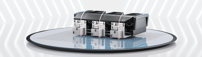
» Parallel Photonic Alignment Engines – Modular. Dynamic. Designed for IC Handlers.