Magnetic Levitation Nanopositioning Stages: 6-DOF Comes Naturally
Technology Demonstrators for Scanning, Hyper Bonding, Metrology
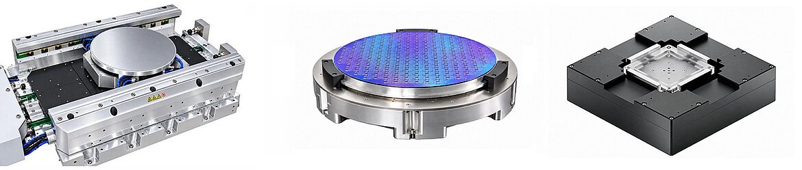
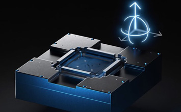
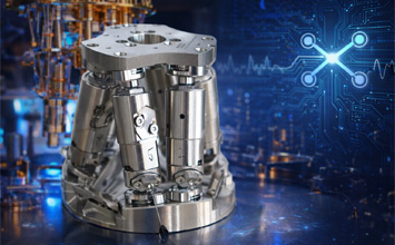
Semiconductor inspection, metrology, and advanced packaging require precise motion across increasingly demanding scan areas and process conditions. PI’s magnetic levitation technology demonstrators combine contact-free motion with active control of all six degrees of freedom: X, Y, Z, and rotation about each axis.
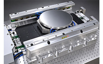
The three platforms address different tasks, from picometer-class AFM scanning over millimeter ranges to long-travel wafer positioning with force control and continuous rotary inspection. Direct actuation allows motion errors to be corrected electronically while eliminating mechanical bearing contact, lubrication, and bearing wear.
Three Platforms for Precision Motion
| Technology demonstrator | Application focus |
| Continuous theta positioning with active rotor plane stabilization | |
| Long-travel linear stage | Wafer positioning, bonding, and dynamic focus tracking |
| AFM scanner | High-resolution surface inspection and metrology over millimeter scan ranges |
Control Motion at the Process Point
Active six-axis control provides a way to correct cross-axis motion, height, and tip/tilt errors within one motion platform. Depending on the demonstrator, it also supports force-controlled bonding, dynamic focus tracking, or programmable stiffness and damping. These capabilities help address measurement stability, settling time, and process consistency without stacking separate motion mechanisms.
These systems are technology demonstrators. Performance values below describe the demonstrated configurations, unless identified as configuration dependent. Final specifications depend on the application and system design.
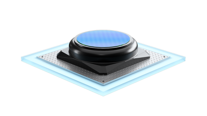
Continuous Rotation with Active Plane Control
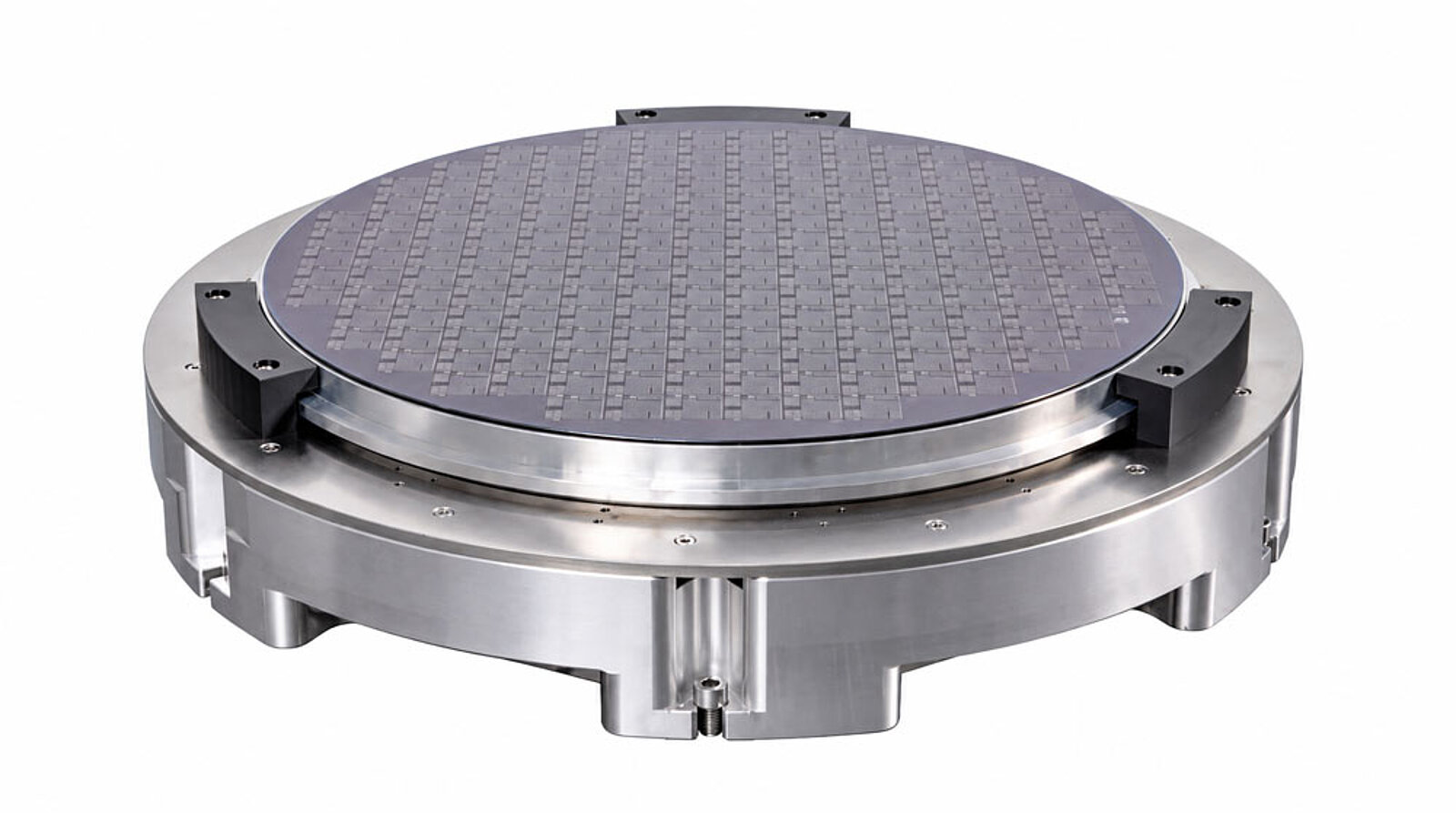
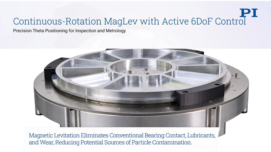
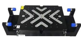
Axial, radial, and tilt errors during rotation can directly affect wafer inspection and metrology. This rotary demonstrator combines unlimited theta travel with active control of the rotor center and plane. Axial position and tip/tilt are stabilized throughout rotation to maintain the measurement plane.
Independent actuation corrects parasitic motion, while repeatable error components can be characterized and compensated electronically. Corrective forces and moments also help suppress vibration, rotor imbalance effects, and process-induced disturbances.
| Demonstrated performance | Value |
| Rotation and speed | Unlimited θZ travel; velocity >600rpm |
| Fine positioning | X/Y: ±200µm; θX/θY: ±0.25mrad |
| Dynamic focus travel | Z: ±600µm |
| In-position stability | Z: 3nm |
| Active plane stability | Axial error: <5nm; non-repeatable error: <3nm RMS; tilt error: <50nrad peak-to-peak |
| Payload | 2kg demonstrated; up to 25kg with other configurations |
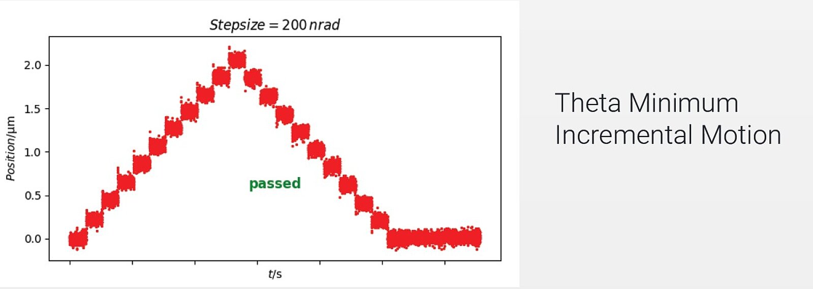
Adapt Rotor Dynamics to the Measurement
Programmable stiffness and damping allow the rotor response to be adapted for dynamic positioning or stable measurement. Contact-free, air-free rotation removes bearing friction, lubricant requirements, and compressed-air infrastructure, including air-pressure-dependent flying height.

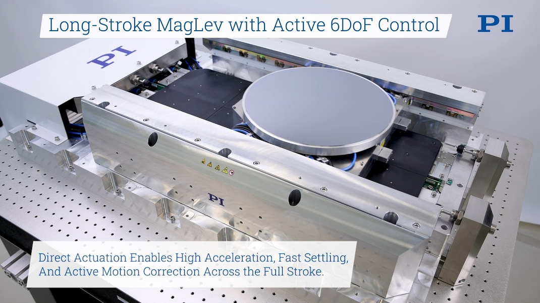
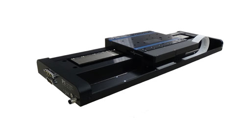
Wafer Positioning and Force Controlled Bonding
Advanced packaging requires accurate alignment, fast positioning, and controlled process forces. This demonstrator integrates long-travel motion, nanometer-class stability, and force control in one levitated body. Low moving mass and direct actuation support high acceleration and short settling times.
Control modes can be selected for individual degrees of freedom, including position control in X/Y and theta, virtual stiffness in tip/tilt, and a constant-velocity Z approach with contact detection and force application. Force and torque monitoring support consistent processing.
| Demonstrated Performance | Value |
| Primary and auxiliary travel | X: 400mm; Y: 400µm; Z: 400µm |
| Angular alignment | θX/θY: 1mrad; θZ: 2mrad |
| Dynamics | Acceleration: 2g (up to 6g possible) velocity: 400mm/s |
| In-position stability | Z: <2nm; θX/θY/θZ: <20nrad |
| Bonding capability | >100N process force; mNforce resolution with an integrated force sensor |
| Repeatability and crosstalk | Double-digit nanometer repeatability; single-digit nanometer XZ/YZ crosstalk over the full Z stroke |

Inspection and Metrology on the Fly
The same long-travel concept supports wafer inspection with active height control during scanning and correction of tip, tilt, and cross-axis errors. The inspection configuration demonstrates Z focus tracking above 200Hz, with <2nm peak-to-peak Z stability and <20nrad peak-to-peak angular stability.
Different configurations can achieve acceleration to 6 g and velocity to 2,000mm/s. Bonding Z travel can reach 2,000µm; the inspection datasheet indicates focus travel of 2,000µm or more with other configurations.
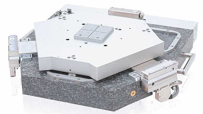
Sub-nanometer Scanning Across Millimeter Ranges
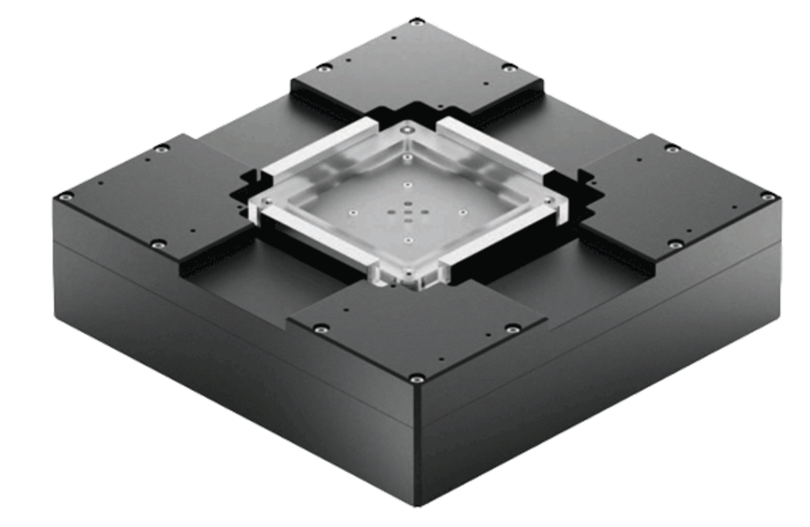
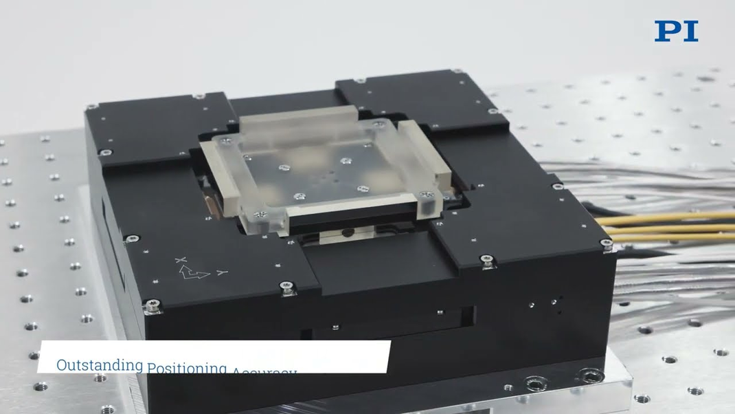
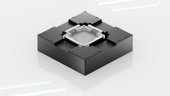
Shrinking semiconductor features and advanced packaging structures require accurate surface measurements over larger fields of view. The MagLev AFM scanner combines ultra-high-resolution, piezo-class motion and millimeter travel in one contact-free stage, supporting picometer scanning resolution and long-range profiling at die level without stitching.
Active six-axis control and iterative learning control (ILC) feed-forward reduce tracking and out-of-plane errors that can distort surface profiles or obscure shallow dishing. Direct actuation supports fast scan turnarounds and site changes without bearing wear or lubrication.
| Demonstrated performance | Value |
| Travel | X/Y: 12.1mm; Z: 50µm; angular motion: 2mrad |
| Resolution | X/Y: ≤50pm; Z: ≤100pm; θX/θY: ≤1.5nrad; θZ: ≤0.5nrad |
| In-position stability | X/Y: <70pm; Z: <110pm |
| Dynamics | Acceleration: 0.15g; velocity: 15mm/s |
| Repeatability and accuracy | <3nm repeatability; <10nm accuracy with calibration |
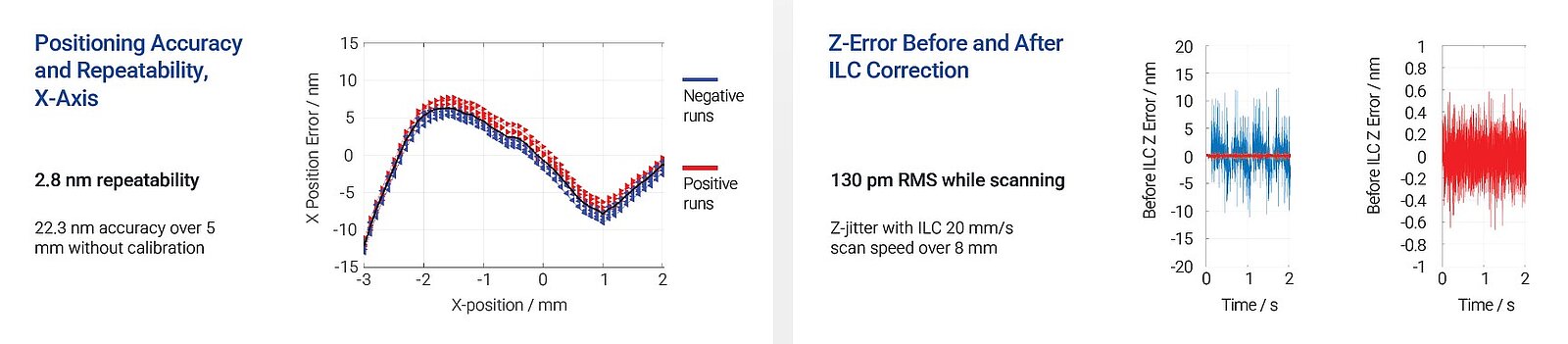
Measured results include 2.8nm X-axis repeatability and 22.3nm accuracy over 5mm without calibration. With ILC, the scanner achieved 130pm RMS Z-jitter at 20mm/s over an 8mm scan.
Other configurations can provide X/Y travel to 50mm, acceleration to 1g, and velocity to 100mm/s. The motion range can be scaled to the application, including wafer-level scanning and profiling.
Discuss Your Application with PI
Whether your process requires high-resolution AFM scans, controlled bonding forces, or continuous rotary inspection, PI can discuss the motion range, payload, stability, dynamics, and control approach needed for your system.
Download precision motion stages for semiconductor test & manufacturing brochure
Talk to a PI expert to discuss your application and request the demonstrator datasheets.




Blog Categories
- Aero-Space
- Air Bearing Stages, Components, Systems
- Astronomy
- Automation, Nano-Automation
- Beamline Instrumentation
- Bio-Medical
- Hexapods
- Imaging & Microscopy
- Laser Machining, Processing
- Linear Actuators
- Linear Motor, Positioning System
- Metrology
- Microscopy
- Motorized Precision Positioners
- Multi-Axis Motion
- NanoAutomation
- Nanopositioning
- Photonics
- Piezo Actuators, Motors
- Piezo Mechanics
- Piezo Transducers / Sensors
- Precision Machining
- Semicon
- Software Tools
- UHV Positioning Stage
- Voice Coil Linear Actuator
- X-Ray Spectroscopy